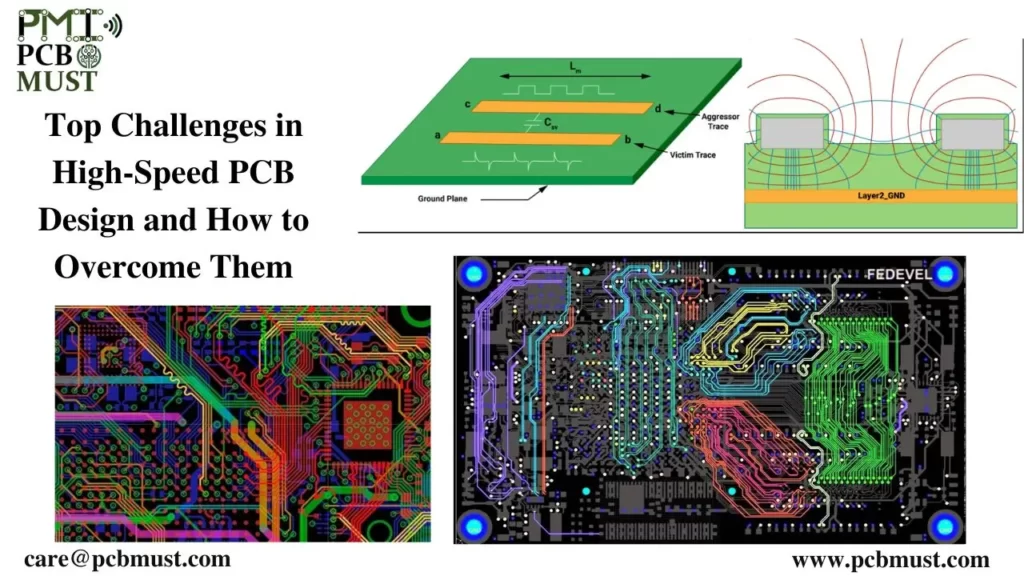
High-speed printed circuit board (PCB) design has become increasingly important in today’s electronics industry. With the rapid development of high-speed digital communication technologies, such as 5G, designing a PCB that can handle high-speed signals has become a major challenge for engineers. In this blog post, we’ll explore some of the top challenges in high-speed PCB design and provide tips on how to overcome them.
Challenge #1: Signal Integrity
Signal integrity is one of the most critical factors in high-speed PCB design. It refers to the ability of a signal to maintain its original quality as it travels along the PCB. High-speed signals are susceptible to interference from noise and crosstalk, which can cause signal degradation and data loss. Therefore, it is crucial to maintain signal integrity throughout the PCB design process.
Solution: To overcome signal integrity issues, designers should focus on careful planning and layout. This includes optimizing the routing, ground and power planes, and decoupling capacitors. Additionally, using a signal integrity simulation tool can help to identify and solve any signal integrity issues before the PCB is fabricated.
Challenge #2: EMI/EMC Compliance
Electromagnetic interference (EMI) and electromagnetic compatibility (EMC) compliance are other major challenges in high-speed PCB design. EMI refers to the unwanted electromagnetic energy that interferes with the performance of electronic devices, while EMC compliance ensures that a device does not emit too much electromagnetic energy that can interfere with other devices.
Solution: To overcome EMI/EMC compliance issues, designers should follow best practices for grounding and shielding, including proper component placement and the use of filtering techniques. Additionally, designers should consider the use of ferrite beads or inductors to suppress high-frequency noise.
Challenge #3: Thermal Management
High-speed PCBs generate a lot of heat due to the high-frequency signals passing through the traces. This can cause components to overheat and fail, leading to reduced performance and reliability.
Solution: To overcome thermal management issues, designers should use thermal visa, thermal pads, and thermal relief pads to dissipate heat away from hotspots. Additionally, designers should consider using a combination of active and passive cooling techniques, such as heat sinks and fans.
Challenge #4: Design for Manufacturing
High-speed PCB design can also present challenges during the manufacturing process. For example, the fine-pitch components and high-density interconnects required for high-speed PCBs can be difficult to manufacture.
Solution: To overcome manufacturing issues, designers should work closely with the manufacturer to ensure that the design is manufacturable. This includes following standard design rules for high-speed PCBs, such as trace width and spacing, and avoiding components that are difficult to place or solder.
In conclusion, designing high-speed PCBs can be challenging, but by focusing on careful planning and layout, following best practices for grounding and shielding, using thermal management techniques, and working closely with the manufacturer, designers can overcome these challenges and create high-performance, reliable PCBs that meet the demands of today’s high-speed digital communication technologies.