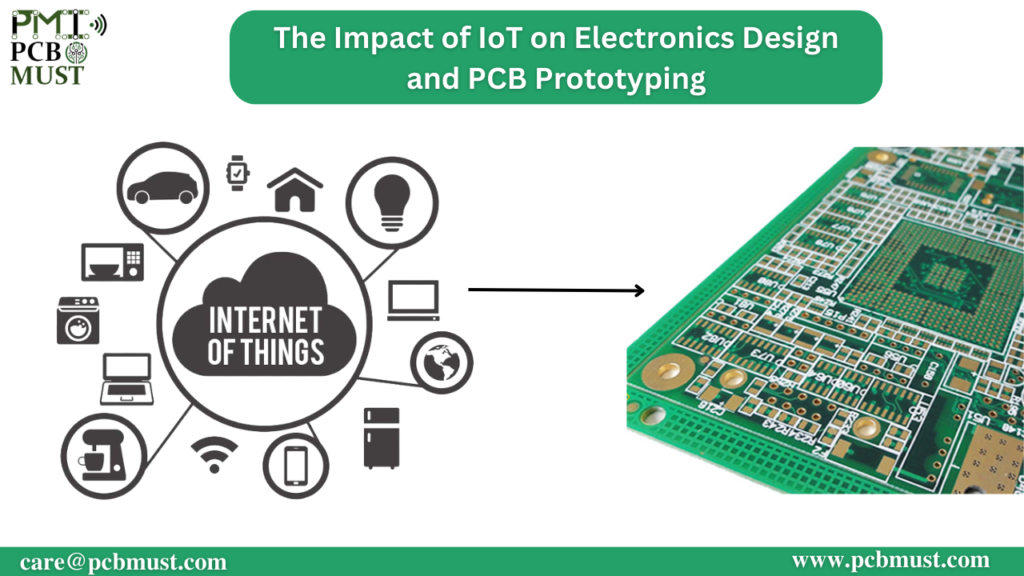
The Internet of Things (IoT) has transformed the way we interact with technology, from wearable devices to smart homes and beyond. As IoT devices become more prevalent, the impact on electronics design and PCB prototyping cannot be ignored. In this article, we will discuss the five key ways IoT is influencing electronics design and PCB prototyping, along with the challenges and solutions for these changes.
Increased Complexity of Electronics Design
- With IoT, the number of components and sensors required in electronic devices has increased significantly, leading to more complex designs. This complexity requires designers to have a more profound understanding of electronics and a higher level of expertise in electronics design. One solution to this problem is to use modular design techniques to break down the complexity of electronics design and make it more manageable.
More Stringent Design Requirements
- IoT devices are often subject to harsh environmental conditions, making it necessary to create electronic devices that can withstand these challenges. This requirement has led to an increase in stringent design requirements, such as high-temperature resistance and moisture-proofing. Designers need to consider these factors when designing IoT devices and use the right materials and components to meet these requirements.
Demand for Miniaturization
- As IoT devices become more integrated into our lives, there is a growing demand for smaller, more compact devices. The smaller the device, the more challenging it becomes to design and manufacture the printed circuit board (PCB) to support it. Designers need to use advanced design techniques to create compact PCBs that meet the performance requirements of IoT devices.
Higher Prototyping Costs
- The complexity of IoT devices and the stringent design requirements have resulted in higher prototyping costs. To address this issue, designers can use simulation and testing software to identify and solve problems in the design stage before moving on to PCB prototyping. This approach can help reduce prototyping costs by minimizing the number of prototypes needed and ensuring that the final design is correct before manufacturing.
Increased Time-to-Market Pressure
- IoT devices are often subject to rapidly changing market demands, meaning that designers and manufacturers need to move quickly to bring products to market. The pressure to reduce the time-to-market has increased significantly in recent years. To meet this challenge, designers need to use the latest tools and technologies, such as rapid prototyping and modular design, to speed up the development process and bring products to market faster.
In conclusion, the impact of IoT on electronics design and PCB prototyping cannot be ignored. The five key ways IoT is influencing electronics design and PCB prototyping are increased complexity, more stringent design requirements, demand for miniaturization, higher prototyping costs, and increased time-to-market pressure. By understanding these challenges and using the right solutions, designers can create innovative and high-performing IoT devices that meet the changing demands of the market.