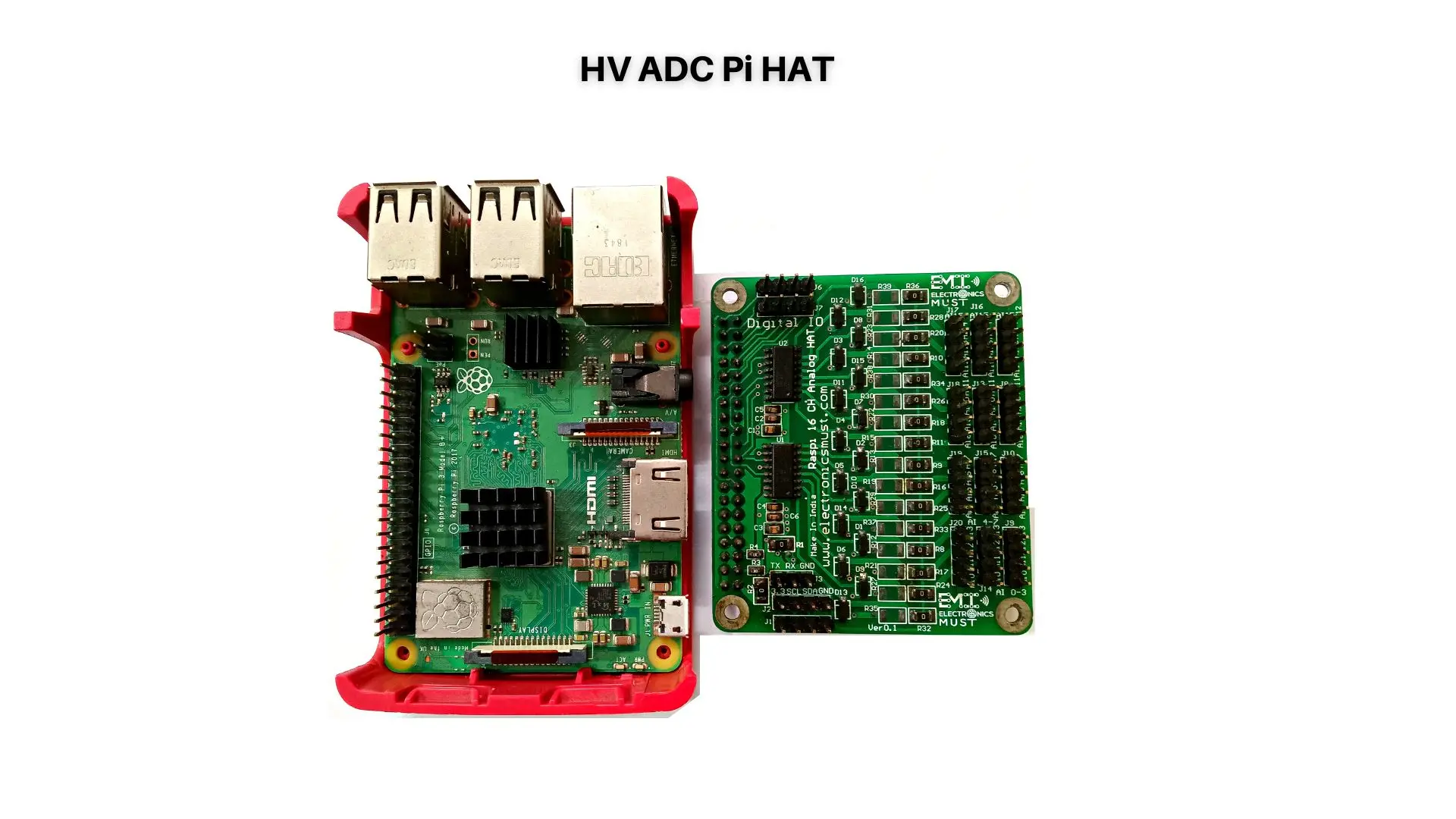
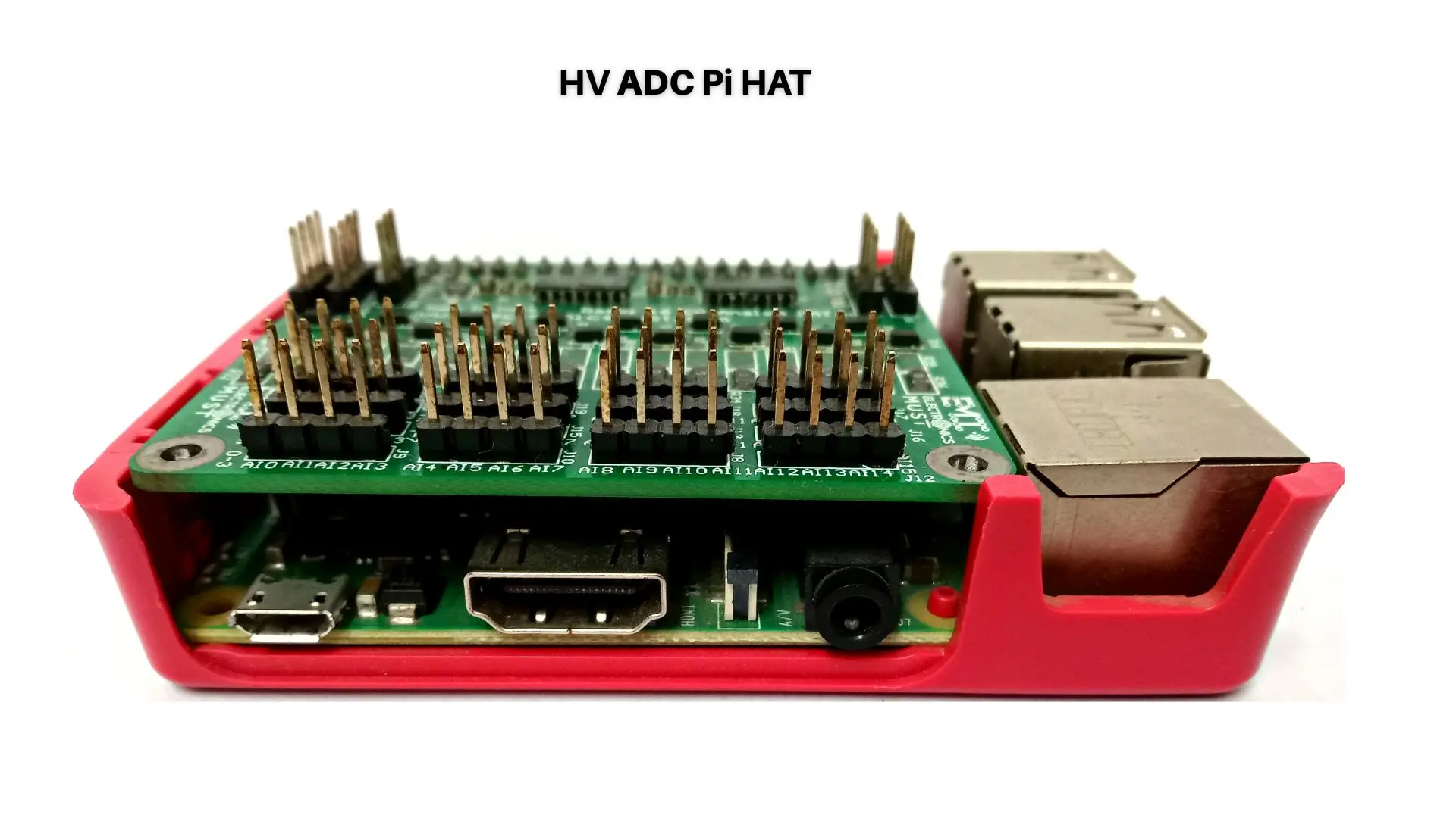
Innovation is the key to success in today’s fast-paced world, particularly in the electronics sector. Companies work hard to develop innovative products that not only satisfy client wants, but also go above and beyond their expectations. Custom PCB design is a key component of achieving this objective. Electronics producers can make their ideas a reality with the help of custom printed circuit boards (PCBs). This article examines the bespoke PCB design process for developing new electronics, stressing its importance and advantages.
The Importance of Custom PCB Design
1. Improving Performance and Functionality
When it comes to enhancing the performance and usefulness of electronic devices, custom PCB design provides flexibility that is unmatched. Custom designs enable accurate component placement, reducing signal interference, and increasing efficiency in contrast to off-the-shelf PCBs. Manufacturers may guarantee that their goods operate to their maximum capacity and provide greater performance to end users by designing the circuitry to meet certain specifications.
2. Minimization and Space Optimisation
Space optimisation is essential in the age of portable and tiny gadgets nowadays. Engineers can create boards that properly fit within the allotted space by using custom PCB design, which eliminates unused spaces. Manufacturers can produce smaller, more streamlined gadgets without sacrificing functionality by reducing the devices’ footprint. This is especially useful in sectors like wearable technology, where size and weight play an important role.
3. Integration and Flexibility in Design
The flexibility needed to incorporate numerous features onto a single board is provided by custom PCB design. Designers can integrate many parts, like microcontrollers, sensors, and wireless modules, into a cohesive system with careful planning and layout. This integration simplifies the production process, increases dependability, and decreases complexity. Additionally, it enables seamless communication between parts, enhancing the functionality of the entire system.
4.Comparability and Scalability
Custom PCB design may cost more up front, but over time, it might result in significant cost savings. Manufacturers can eliminate pointless components and lower production complexity by adapting the design to unique needs. Additionally, since custom PCBs can be tailored for automated assembly, production labour costs will be lower. Additionally, as the product’s demand rises, custom designs offer scalability, allowing for efficient mass production.
The Process of Custom PCB Design
1. Analysis and Conceptualization of Requirements
Thorough requirement analysis is the first step in the process of turning an idea into reality. Manufacturers and design engineers collaborate closely to specify the needed features, performance objectives, and limits. Ideas are conceptualised and rough design sketches are made during this stage. The basis for the following steps is laid by this collaborative approach, which guarantees a clear grasp of the project’s goals.
2. Component selection and schematic design
Making a schematic diagram is the next step after defining the criteria. The circuit’s logical representation is captured in the diagram, which also shows how the components are connected to one another. Design engineers make meticulous component selections based on their criteria to guarantee performance and compatibility. The selection process takes into account elements including power requirements, signal integrity, and environmental concerns.
3. PCB Routing and Layout
Following completion of the schematic design, attention turns to PCB layout and routing. To place and route the components on the board, design engineers use specialised software. During this phase, variables like signal integrity, thermal management, and manufacturability are taken into account. Designers can optimise the positioning to reduce signal interference and achieve the desired form factor thanks to advanced technologies.
4. Testing and prototyping
A prototype is created after the PCB layout is finished. The design can be thoroughly tested and validated through prototyping. The prototype is put through a number of tests, including evaluations of its performance, dependability, and functionality. Based on the test results, any necessary adjustments or improvements are made to guarantee the design satisfies the required requirements.
5. Production and Manufacturing
The manufacturing stage starts as soon as the prototype design is complete. Following industry standards and quality control methods, custom PCBs are produced. This often entails actions like applying solder paste, mounting components, soldering, and inspecting. Depending on the design specifications, advanced manufacturing methods like surface mount technology (SMT) and through-hole mounting are used.
6.Design Rule Check (DRC)
A design rule check is done to make sure the PCB design complies with the manufacturing capabilities and requirements before moving on with manufacture. Potential problems like spacing violations, trace width violations, and other design rule breaches can be found using this step.
7. Product integration and assembly
The finished product incorporates the PCBs after they have been produced. In order to construct a working electronic gadget, additional parts including screens, enclosures, and connectors are put together at this step. At every stage of the assembly process, stringent testing and quality control procedures are carried out to make sure the product fulfils the desired specifications and performance criteria.
8.Generation of Gerber Files:
The design files are transformed into Gerber files once the PCB design is complete and passes the DRC. The PCB layers, copper traces, component placements, drill holes, and other design specifics are all included in the Gerber files. These documents are necessary for the production process.
9.Bill of Materials (BOM):
A thorough BOM is generated, outlining every part needed for PCB assembly. Part numbers, component descriptions, quantity breakdowns, and supplier details are all included in the BOM. It acts as a procurement guide and guarantees the availability of all required parts.
Conclusion
Innovative electronics must be developed via custom PCB design in order to become a reality. Manufacturers may optimise functionality, improve performance, and produce distinctive goods that stand out in the market by taking use of the benefits of custom designs. Custom PCB design comprises a number of steps, from requirement analysis to product assembly, each of which is important to the project’s success as a whole. Companies can stay ahead of the competition, provide outstanding user experiences, and revolutionise the electronics industry by embracing custom PCB design.


