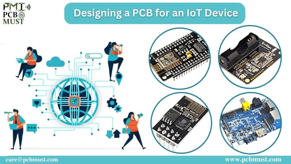
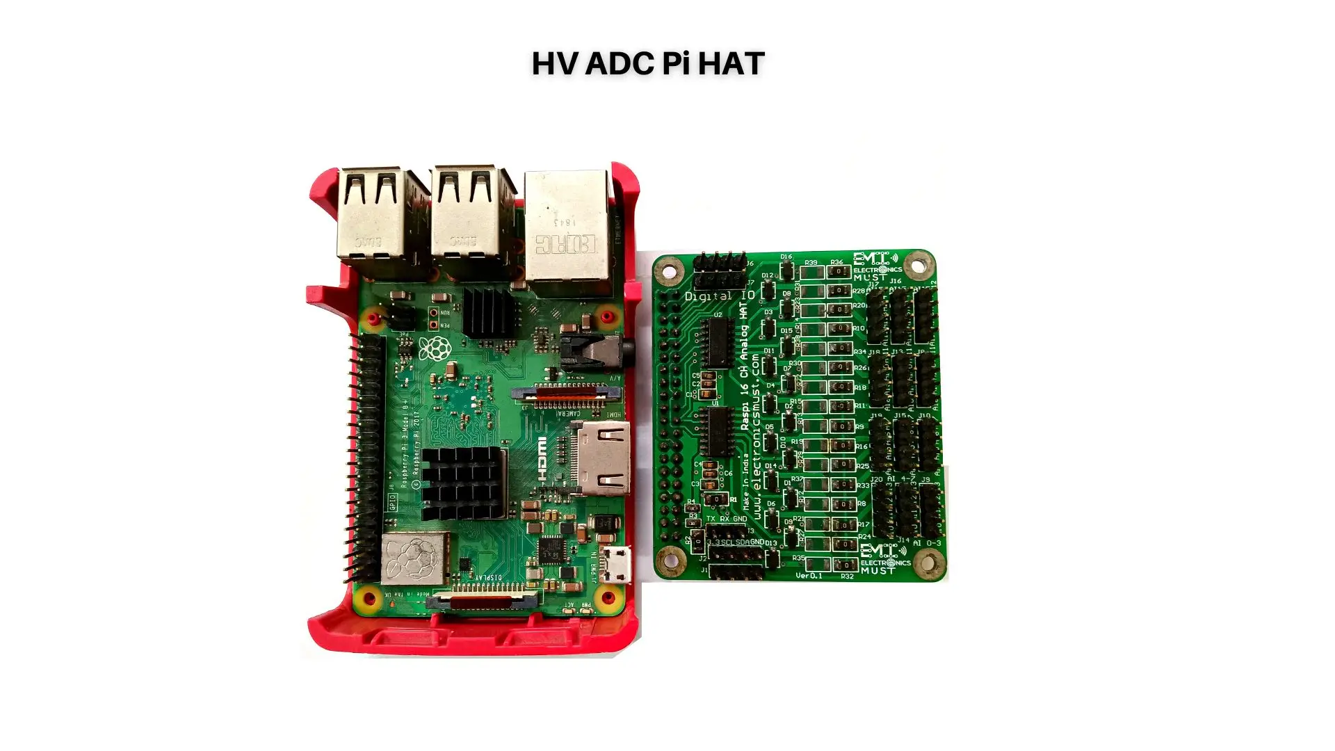
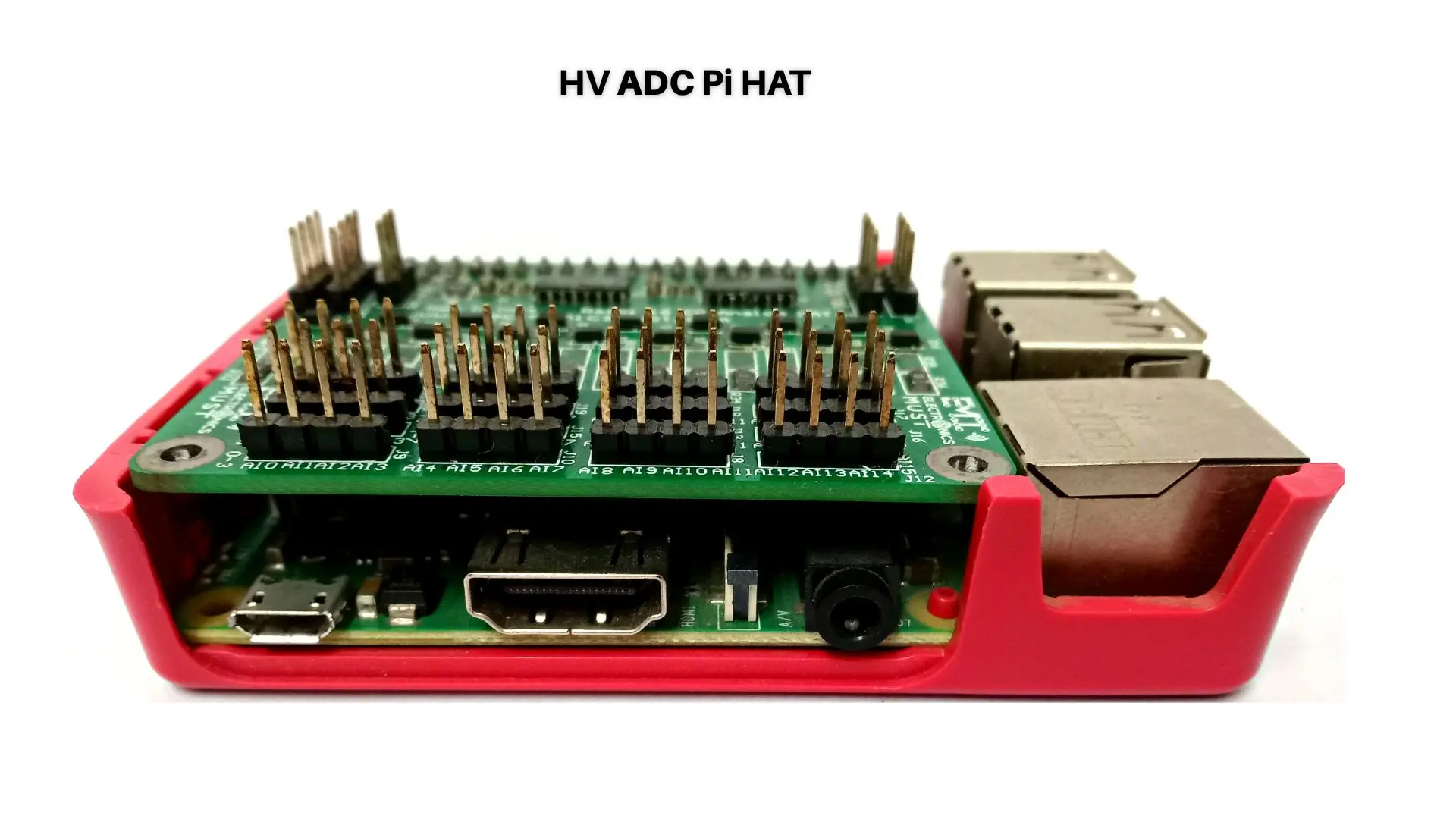
The Internet of Things (IoT) is rapidly transforming the way we live, work, and interact with technology. The vast network of connected devices has opened up new possibilities for data collection, analysis, and control. A key component of IoT devices is the Printed Circuit Board (PCB), which acts as the backbone for these devices, connecting all the components and enabling communication. In this case study, we will explore the process of designing a PCB for an IoT device, highlighting the important considerations and challenges involved.
Understanding the Requirements
The first step in designing a PCB for an IoT device is to understand the requirements. This includes identifying the components that need to be included on the board, such as microcontrollers, sensors, communication modules, and power management components. The size and form factor of the device must also be considered, as well as the power requirements and communication protocols. All of these requirements will influence the size and shape of the PCB, as well as the number and type of components that need to be included.
Layout Design
Once the requirements have been defined, the next step is to design the layout of the PCB. The layout must be designed to ensure that all components fit within the available space and that there is enough clearance between components to prevent any short circuits or interference. In addition, the layout must be designed to accommodate the routing of the electrical signals between components, including power, data, and control signals. This process requires careful consideration of signal integrity and power distribution, as well as the routing of signals to minimize interference and signal loss.
Component Selection
The next step is to select the components that will be used on the board. This includes selecting the microcontroller, sensors, communication modules, and power management components. The selection of components must be based on their compatibility with the requirements of the device, as well as their cost and availability. The components must also be selected based on their reliability and performance, as this will directly impact the overall reliability and performance of the device.
Manufacturing and Testing
Once the PCB design has been finalized, it must be manufactured and tested. The manufacturing process involves the creation of the physical board, including the etching of the copper tracks, drilling of the holes for the components, and the application of the solder mask and silkscreen. The testing process involves verifying that the board functions as expected and that all components are properly connected and communicating with each other. This includes functional testing, performance testing, and environmental testing to ensure that the device will operate reliably in a wide range of conditions.
Designing a PCB for an IoT device is a complex and challenging process, requiring careful consideration of the requirements, layout design, component selection, and manufacturing and testing. By following a rigorous process and paying attention to the important details, it is possible to create a high-quality and reliable PCB that will enable the full potential of IoT. With the right design, an IoT device can provide new insights, control, and efficiency, revolutionizing the way we live, work, and interact with technology.


